There are no items in your cart
Add More
Add More
| Item Details | Price | ||
|---|---|---|---|

Instructor: SemioncsLanguage: English
About the Course:
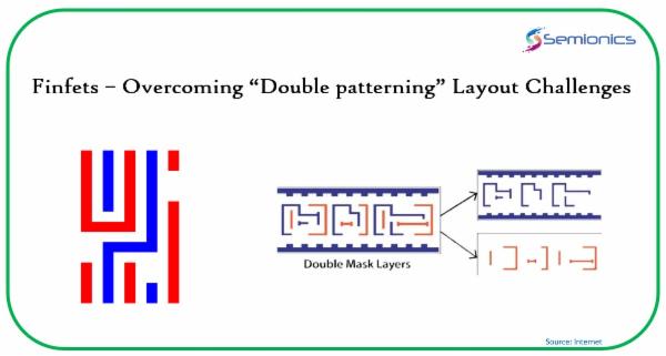
This Session is mainly created to address the issues and workarounds in Overcoming “Double patterning” Layout Challenges in finfets. It explains the concept and need of Double patterning. The explanation revolves around references from TSMC 7nm.Handling tricky DRCs and the precautions a layout engineer needs to take to avoid Double patterning related DRCs and density issues. The session also mentions about challenging issues and mitigation methods are discussed in this session. Some tips and tricks which would help the aspiring Engineers to improve their layout skills. and do their job in an organized way to become an Efficient layout engineer.
Who can Benefit from this course?
- Undergrad students, Master's Students, PHD candidates, Faculties, technology enthusiasts, Job seekers, it would help in interview preparation
- Working Professionals who would want to enhance their skill in profiles like (ASIC design, Analog Circuit Design, Analog IC layout Design, Physical Design, Physical Verification, Standard cell Layout Design, Analog Layout Design, Memory Layout Design & IO Layout Design).
- Things what you learn in this session, would help you improve the quality of work what you deliver.
- Candidates who are hungry for Knowledge and would want to know the Whole ASIC implementation.
The topics covered are as below:
- What is Double patterning?
- Why do we go for Double patterning?
- Types of patterning trends
- Double Patterning metals & Vias
- Double patterning DRC issues
- Addressing G0 errors
- Double patterning Density issues
- Balancing the colours
- Addressing Line Edge density issues
Just starting out? No need to worry. Let’s take the first step together.
Pick up a new skill and learn why practice makes perfect.
Stuck on something? Discuss it with your peers in your virtual classroom.
Learn what makes you tick and how you can use it to your benefit.
 Launch your Graphy