There are no items in your cart
Add More
Add More
| Item Details | Price | ||
|---|---|---|---|


Language: English
About the Courses:
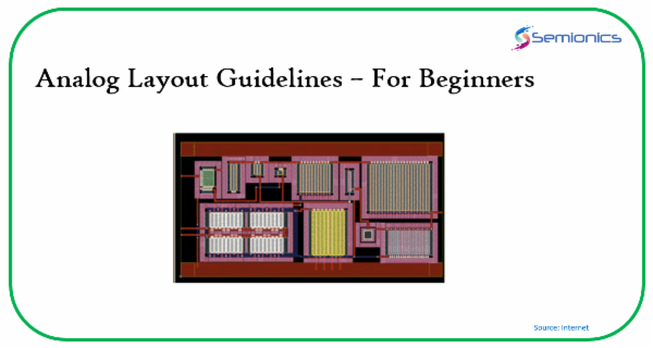
This is a package of 2 courses, teaching you the details of Planar and Finfet Layout guidelines. It is mainly designed for working professionals who want to explore about Finfet Layouts. Even the beginners can get the feel and understanding of How different is Finfet from Planar CMOS? Since we have extensive expertise of working on finfets. we tend to share the knowledge of Do’s and Don’ts when you are working with finfet Layouts. Finfet Layouts when done in a methodical way can be done quicker avoiding the nightmare a layout engineer would face with DRCs.
A proper approach on finfet layout guidelines is covered in this session trying to cover almost all the important DRCs which could form a bottleneck during your Tape-outs. We have also covered about Double patterning concepts. the precautions one needs to take to avoid getting into Max POLY density issue. Taking care of these things will certainly help you meet your deadlines
Note: When you click on the individual courses, you would get the details of what’s being covered in the sessions
Who can Benefit from this course?
- Working Professionals who would want to enhance their skill in profiles like (ASIC design, Analog Circuit Design, Analog IC layout Design, Physical Design, Physical Verification, Standard cell Layout Design, Analog Layout Design, Memory Layout Design & IO Layout Design).
- Undergrad students, Master's Tech Students, PHD candidates, Faculties, technology enthusiasts, Job seekers, it would help in interview preparation
Just starting out? No need to worry. Let’s take the first step together.
Pick up a new skill and learn why practice makes perfect.
Stuck on something? Discuss it with your peers in your virtual classroom.
Learn what makes you tick and how you can use it to your benefit.
 Launch your Graphy
